








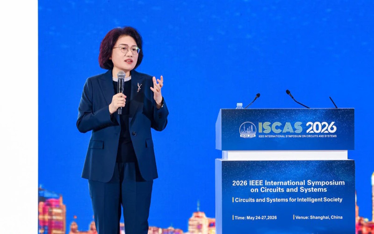
During a keynote in Shanghai at the International Symposium of Circuits and Systems (ISCAS), Huawei revealed some of the advancements the company made in the past six years, talked about a new architecture that would solve current chip manufacturing constraints and even proposed a new scaling law to replace the dated Moore’s Law.
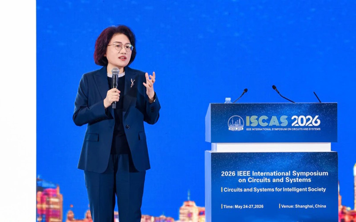
Moore’s Law has been around for more than five decades now and has shaped the chip manufacturing industry. Still, lately, it has been facing physical limits and diminishing economic returns, partially because it’s based on geometric scaling. Huawei came up with a new scaling law called “Tau (τ) Scaling Law.” It’s based on time, and Huawei believes it’s the way to go when it comes to semiconductor industry development.
Interestingly enough, Huawei has already mass-produced 381 chips used in a wide range of industries based on the Tau Scaling Law.
Thanks to the new scaling law, Huawei also developed a new LogicFolding architecture that continuously compresses signal propagation delay and improves transistor density in semiconductors. The architecture is applicable not just to semiconductors but circuits, systems and other types of chips.
Huawei’s next-generation 2026 Kirin chips for smartphones will be the first to adopt the LogicFolding architecture, which is expected to boost performance significantly over the previous generations. The first chips will hit the market this fall.
Huawei also promises high-end Huawei chips in 2031 to feature transistor density equivalent to 1.4nm chips.
The Chinese tech giant also reached out to partners worldwide, stating that openness and collaboration are the way to go forward, and no single company will be able to solve all the technical limitations that arise with semiconductor evolution.